






Published Date: July 29, 2026
Last Updated: July 29, 2026
Author: Felix Lee, CEO at Forgecise
Table of Contents
Felix Lee is the CEO at Forgecise, focusing on advanced manufacturing technologies and industrial production solutions. His work covers the connection between ceramic additive manufacturing, engineering applications, and next-generation semiconductor technologies.
Through his experience with advanced manufacturing systems, Felix Lee focuses on how material choices and production methods influence component performance, design flexibility, and industrial scalability.
Quick Answer
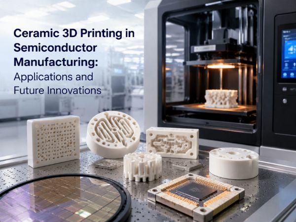
Ceramic 3D printing in semiconductor manufacturing allows companies to produce high-performance ceramic components with precise dimensions, complex structures, and customized properties. The technology supports semiconductor packaging, heat management, microelectronic structures, and specialized manufacturing tools by solving many limits found in traditional ceramic processing.
TL;DR: Key Points
- Ceramic materials such as silicon nitride (Si₃N₄), aluminum oxide (Al₂O₃), and zirconia (ZrO₂) are widely used in semiconductor applications because of their heat resistance, insulation, and mechanical strength.
- Ceramic 3D printing technologies, including DLP and SLA, allow engineers to create complex ceramic parts with micron-level accuracy.
- Main applications include semiconductor packaging, thermal management systems, microelectronic structures, sensors, and customized production tools.
- Current challenges include material development, sintering quality, production speed, and manufacturing cost.
- As the technology improves, ceramic 3D printing may become a larger part of semiconductor production.
Why Are Ceramic Materials Important in Semiconductor Manufacturing?
Ceramic materials are important in semiconductor manufacturing because modern electronic devices need materials that can handle high temperatures, electrical stress, and demanding production environments.
Semiconductor industries produce increasingly smaller and more powerful devices. Integrated circuits (IC), microelectronics, sensors, and high-power electronic systems all require materials that can maintain stable performance.
Traditional materials may struggle when devices operate at higher power levels or extreme temperatures. Ceramic materials provide a combination of properties that make them suitable for these applications.
Key advantages include:
- High temperature resistance
- Strong electrical insulation
- Corrosion resistance
- Mechanical durability
- Thermal management capability
These characteristics make ceramics useful in semiconductor equipment, packaging systems, and precision components.
What Ceramic Materials Are Used in Semiconductor Applications?
Several ceramic materials are commonly used in semiconductor manufacturing. Each material provides different advantages depending on the application.
| Ceramic Material | Main Properties | Semiconductor Uses |
|---|---|---|
| Aluminum Oxide (Al₂O₃) | Electrical insulation and stable performance | Insulating components and semiconductor parts |
| Zirconia (ZrO₂) | High strength and wear resistance | Durable ceramic components |
| Silicon Nitride (Si₃N₄) | Excellent thermal performance and mechanical strength | Packaging, cooling systems, and high-power electronics |
How Do Ceramics Support Semiconductor Devices?
Thermal Management Components
Heat is one of the biggest challenges in modern semiconductor systems.
High-power chips and electronic devices generate large amounts of heat during operation. If heat is not controlled, device performance and reliability can decrease.
Ceramic materials help manage heat because they can maintain their properties under high-temperature conditions.
Applications include:
- High-power semiconductor devices
- Laser systems
- LED components
- High-frequency electronic equipment
Electrical Insulation Components
Semiconductor devices require reliable electrical separation between different components.
Ceramics provide excellent insulation performance, making them suitable for:
- Semiconductor packaging
- Isolation structures
- Electronic protection components
High-Temperature Components
Many semiconductor manufacturing processes require high-temperature environments.
Examples include:
- Wafer processing
- Thin-film deposition
- Other advanced semiconductor production steps
Ceramic materials can maintain stability in these conditions.
How Does Ceramic 3D Printing Improve Semiconductor Manufacturing?
Traditional ceramic manufacturing methods have supported semiconductor production for many years. However, they often face challenges related to precision, production speed, and design flexibility.
Manufacturing ceramic components traditionally may require:
- Custom molds
- Multiple processing steps
- Long production cycles
- Limited design options
Ceramic 3D printing provides a different approach. Instead of removing material through machining, additive manufacturing builds components layer by layer based on digital designs.
This allows engineers to create parts that are difficult to produce using conventional methods.
What Are the Main Benefits of Ceramic 3D Printing Technology?
High Precision Manufacturing
One major advantage of ceramic 3D printing is its ability to create highly accurate components.
Technologies such as:
- Digital Light Processing (DLP)
- Stereolithography (SLA)
can achieve micron-level precision.
This precision is valuable for semiconductor applications where small dimensional differences can affect component performance.
Examples include:
- Micro-scale structures
- Precision ceramic components
- Complex semiconductor parts
Faster Prototype Development
Traditional ceramic manufacturing often requires tooling and mold preparation before production begins.
Ceramic 3D printing shortens this process.
Engineers can:
- Design a component digitally
- Print a prototype
- Test performance
- Modify the design
This faster development process helps companies evaluate new semiconductor components more efficiently.
Complex Structure Manufacturing
Some ceramic structures are difficult to create using traditional manufacturing.
Ceramic 3D printing allows the production of:
- Internal channels
- Porous ceramic structures
- Micro-scale geometries
- Complex cooling designs
These structures can improve performance by allowing better heat control and more efficient component designs.
Customized Ceramic Materials
Ceramic 3D printing also supports material customization.
Manufacturers can adjust ceramic formulations based on specific requirements.
Customization may focus on:
- Thermal performance
- Electrical characteristics
- Mechanical strength
- Environmental resistance
This flexibility helps engineers develop ceramic components for specific semiconductor applications.
What Are the Main Applications of Ceramic 3D Printing in Semiconductor Manufacturing?
Ceramic 3D printing is being applied in several important semiconductor areas.
1. Semiconductor Packaging and Thermal Management Solutions
Semiconductor packaging is one of the most important applications for ceramic 3D printing.
As semiconductor devices become more powerful, managing heat becomes more difficult.
Traditional packaging materials, including aluminum and silicon-based solutions, may have limitations when operating under high temperatures and high power conditions.
Ceramic 3D printing provides packaging components with:
- Strong thermal stability
- Electrical insulation
- Resistance to high temperatures
Silicon nitride ceramic (Si₃N₄) is especially valuable because it combines heat performance with mechanical strength.
Applications include:
- High-power laser packaging
- LED devices
- High-frequency electronic systems
For advanced semiconductor products, better thermal management can help maintain stable operation.
2. Precision Structures for Microelectronic Devices
Modern semiconductor manufacturing requires extremely small and accurate structures.
Ceramic 3D printing allows engineers to create micro-scale designs that traditional processing methods may not easily produce.
Applications include:
- Integrated circuit (IC) manufacturing structures
- Microfluidic channels
- Sensor components
- Cooling structures
Microfluidic ceramic channels can support:
- Chip cooling systems
- Chemical processing applications
- Sensor development
These structures provide more design options for future semiconductor devices.
3. Customized Semiconductor Manufacturing Tools and Molds
Semiconductor production often requires specialized tools and components.
Traditional ceramic manufacturing can become difficult when companies need:
- Small production quantities
- Custom designs
- Fast engineering changes
Ceramic 3D printing provides a flexible method for creating these components.
Applications include:
- Wafer processing tools
- Laser etching components
- Micro and nano structure production equipment
The main benefits include:
- Faster development
- Lower prototype costs
- More design freedom
What Challenges Does Ceramic 3D Printing Still Need to Solve?
Although ceramic 3D printing has strong potential in semiconductor manufacturing, several technical challenges remain.
Material System Development
Ceramic 3D printing materials continue to improve.
Current research areas include:
- Better ceramic formulations
- Wider material choices
- Improved printing performance
More advanced materials will help expand industrial applications.
Sintering and Final Performance
After printing, ceramic components usually require a sintering process to achieve final strength and performance.
Manufacturers need better control over:
- Density
- Mechanical strength
- Electrical properties
- Reliability
Semiconductor applications require very stable and consistent component performance.
Production Speed and Cost
Today, many ceramic 3D printing applications focus on:
- High-value parts
- Custom components
- Small-batch production
Future improvements need to focus on:
- Faster printing processes
- Lower manufacturing costs
- Larger production capacity
What Is the Future of Ceramic 3D Printing in Semiconductor Manufacturing?
The future of ceramic 3D printing is closely connected with the development of advanced semiconductor technologies.
As semiconductor devices become:
- Smaller
- More powerful
- More demanding in thermal performance
manufacturers will need better materials and more flexible production methods.
Ceramic 3D printing may expand from specialized applications into broader semiconductor manufacturing.
Future opportunities include:
Advanced Semiconductor Packaging
Ceramic materials may support future:
- AI chips
- High-power electronics
- Advanced computing devices
Better Thermal Management Designs
3D printed ceramic structures may improve cooling solutions through:
- Internal channels
- Optimized geometries
- Customized thermal properties
Next-Generation Manufacturing Tools
Ceramic additive manufacturing may help produce:
- Advanced semiconductor components
- Customized manufacturing equipment
- High-performance electronic structures
The combination of ceramic materials and 3D printing gives semiconductor engineers new options for solving future manufacturing challenges.
Frequently Asked Questions About Ceramic 3D Printing in Semiconductor Manufacturing
What is ceramic 3D printing used for in semiconductor manufacturing?
Short Answer:
Ceramic 3D printing is used to create semiconductor packaging parts, thermal management components, microstructures, and customized manufacturing tools. It helps engineers produce ceramic components with high precision, complex designs, and strong thermal and electrical performance.
Ceramic 3D printing is especially useful when traditional ceramic manufacturing cannot easily produce the required shape or level of customization.
Why are ceramics used in semiconductor devices?
Short Answer:
Ceramics are used because they provide heat resistance, electrical insulation, corrosion resistance, and mechanical strength. These properties help semiconductor components operate reliably in high-temperature and high-performance environments.
Ceramic materials are commonly used in packaging systems, insulation parts, and manufacturing equipment.
Which ceramic materials are commonly used in semiconductor applications?
Short Answer:
The main ceramic materials include aluminum oxide (Al₂O₃), zirconia (ZrO₂), and silicon nitride (Si₃N₄). Each material provides different benefits, such as insulation, strength, or thermal performance.
Silicon nitride is especially useful for high-power electronic applications because of its excellent thermal properties.
How does ceramic 3D printing improve semiconductor production?
Short Answer:
Ceramic 3D printing improves semiconductor production by enabling faster prototyping, complex structures, and precise component manufacturing. Technologies such as DLP and SLA allow engineers to create detailed ceramic parts with micron-level accuracy.
This gives manufacturers more flexibility when developing advanced semiconductor systems.
Can ceramic 3D printing support large-scale semiconductor production?
Short Answer:
Ceramic 3D printing has the potential to support larger semiconductor production in the future, but improvements are still needed in printing speed, cost, material systems, and manufacturing reliability.
The technology currently works best for specialized and high-value components.
About Forgecise
Forgecise focuses on advanced manufacturing solutions and emerging production technologies. Through research and engineering applications, Forgecise follows how ceramic additive manufacturing can support industries that require precision, reliability, and advanced material performance.
Author: Felix Lee, CEO at Forgecise
Last Updated: July 29, 2026
Note: This article provides general industry information about ceramic 3D printing and semiconductor manufacturing. Specific component designs and production decisions should be evaluated based on engineering requirements and industry standards.