





By Felix Lee | CEO at Forgecise
Table of Contents
Published on June 12, 2026 • Reading Time: 8 min (~1,700 words) Reviewed by: Additive Manufacturing & Microelectronics Editorial Team
Fast Answer Box
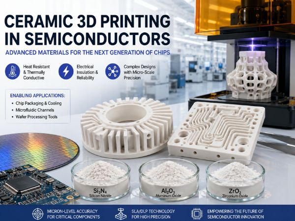
What is ceramic 3D printing in the semiconductor industry? > It is an additive manufacturing process—mainly using SLA and DLP light techniques—that builds high-precision ceramic parts layer by layer for microchips, power electronics, and sensors.
Why is it useful for chip makers? > Hard ceramic materials are difficult to cut or drill with old tools. 3D printing lets engineers print micro-scale cooling channels, light molds, and heat-resistant holders using materials like Silicon Nitride (\text{Si}_3\text{N}_4), Aluminum Oxide (\text{Al}_2\text{O}_3), and Zirconium Oxide (\text{ZrO}_2).
Introduction
Microchips, integrated circuits (ICs), and sensors are getting smaller and more powerful every year. As electronics shrink, they run hotter and push materials to their limits. Semiconductor factories need tough materials that can block electricity, handle extreme heat, and resist harsh chemicals.
Technical ceramics fit these needs well. But making ceramic parts with standard factory tools is hard. Ceramic blocks are stiff and brittle. Cutting them takes a long time, costs too much money, and ruins delicate designs.
3D printing offers a practical solution. By building parts layer by layer from digital models, 3D printing gives engineers new ways to make precise ceramic parts.
This guide breaks down how ceramic 3D printing works in chip manufacturing, the top materials used, three real applications, and the main challenges ahead. Our analysis builds on industry data published by the Shenzhen 3D Printing Association and technical teams at Qiyu Technology (ADTE).
Why Semiconductors Need Technical Ceramics
Ceramics perform tasks that metals and plastics cannot handle inside a semiconductor plant or chip package.
+-------------------------------------------------------------------+
|               KEY CERAMIC PROPERTIES IN SEMICONDUCTORS           |
+-------------------------------------------------------------------+
|  1. Heat Control: Moves heat away quickly to prevent damage.      |
|  2. Electrical Block: Stops electric currents from leaking.       |
|  3. Heat Resistance: Survives hot chip-making steps without warping.|
|  4. Chemical Resistance: Stands up to harsh etching acids and gas. |
+-------------------------------------------------------------------+
The Three Main Ceramic Materials
Semiconductor equipment relies on three major technical ceramics:
- Aluminum Oxide (\text{Al}_2\text{O}_3): This is the most common choice. It insulates against electricity, stays strong under pressure, and keeps production costs low. Factories use it for simple substrates and isolation plates.
- Zirconium Oxide (\text{ZrO}_2): Known for high strength and wear resistance. It works best in mechanical parts that face high physical friction or stress.
- Silicon Nitride (\text{Si}_3\text{N}_4): The top performer for severe heat conditions. It combines high thermal conductivity with strong resistance to sudden temperature changes.
Where Ceramics Fit in Chip Production
- Heat Management: Power devices generate large amounts of heat. Ceramic heat sinks pull thermal energy away to keep chips stable.
- Electrical Insulation: Ceramics separate live circuits inside electronic packages to stop electrical shorts.
- High-Temperature Parts: Processing steps like wafer handling, chemical vapor deposition (CVD), and thin-film deposition run at high temperatures. Ceramic components withstand these spaces without changing shape.
The Main Problem with Traditional Ceramic Machining
Although ceramics have great traits, old manufacturing methods create heavy bottlenecks. Once ceramic powder is fired into a solid block, it becomes almost as hard as diamond.
OLD CERAMIC MACHINING                  CERAMIC 3D PRINTING
+-------------------------------+      +-------------------------------+
| * Requires hard molds         |      | * Prints straight from CAD    |
| * High cost for small runs    |  VS  | * Fast design tweaks          |
| * Simple shapes only          |      | * Complex hollow channels     |
| * Hard to make tiny features  |      | * Micron-level details        |
+-------------------------------+      +-------------------------------+
Four Limits of Standard Methods
- Low Precision for Micro Features: Cutting tools cannot easily carve sub-millimeter structures into hard ceramic blocks without breaking them.
- Long Production Times: Making metal molds for traditional ceramic casting often takes weeks or months. This slows down test cycles.
- Restricted Designs: Drill bits move only in straight lines. They cannot drill curved internal cooling channels inside a solid ceramic block.
- High Costs for Custom Parts: Creating a few custom ceramic parts using traditional tools costs too much money per piece.
How Ceramic 3D Printing Works
3D printing removes the need for physical molds. Instead of carving material away, a 3D printer reads a computer design file and prints the part step by step.
                       CERAMIC 3D PRINTING PROCESS

 [ CAD File ] ---> [ Resin & Powder Liquid ] ---> [ Light Curing (SLA/DLP) ]
                                                           |
                                                           v
 [ Dense Solid Part ] <--- [ Oven Heating / Sintering ] <--- [ Soft Printed Part ]
Core Methods: DLP and SLA
The semiconductor sector mostly relies on light-based methods: Digital Light Processing (DLP) and Stereolithography (SLA).
First, technicians mix fine ceramic powder into a liquid resin that reacts to light. A projector or UV laser shines light onto the liquid layer, hardening the resin and trapping the ceramic powder.
Once the shape is fully printed, the part goes into a high-heat oven (sintering furnace). The heat burns off the resin binder and melts the ceramic particles into a solid, dense part.
Four Advantages for Electronics
- Micron Accuracy: DLP printers control features down to the micron scale, meeting tight tolerances needed for microchips.
- Fast Testing: Designers update a CAD file, start the printer, and test a real ceramic part in a few days.
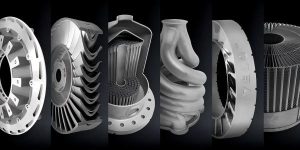
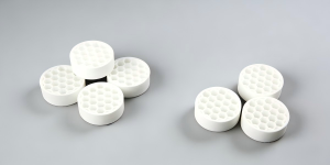
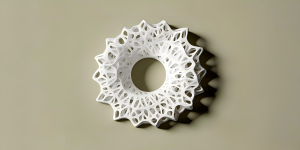
- Complex Geometry: 3D printers can form open lattice patterns, multi-porous ceramic samples, and hollow internal paths effortlessly.
- Custom Material Blends: Chemical teams can tweak the liquid mix to alter heat flow, electrical limits, or strength for specific applications.
3 Real Applications in the Semiconductor Sector
Data from Shenzhen 3D Printing Association reports show that hardware companies are applying 3D printed ceramics in three core areas.
       +---------------------------------------------------------+
       |     3 USES FOR 3D PRINTED CERAMICS IN SEMICONDUCTORS    |
       +---------------------------------------------------------+
       |                                                         |
       |  [1] Chip Packaging & Cooling                           |
       |      - High-Power Lasers, LEDs, High-Frequency Gear     |
       |      - Silicon Nitride (Si3N4) Heat Sinks               |
       |                                                         |
       |  [2] Tiny Structures & Liquid Cooling                   |
       |      - Microfluidic Channels Inside Chips               |
       |      - Mini Chemical Reactors & Precision Sensors       |
       |                                                         |
       |  [3] Custom Tools & Wafer Equipment                     |
       |      - On-Demand Wafer Processing Fixtures              |
       |      - Custom Laser-Etching Molds                       |
       +---------------------------------------------------------+
1. Chip Packaging and Heat Dissipation
Standard microchip packages often use aluminum metal or silicon plates. But high-power chips—like industrial lasers, LED setups, and high-frequency communication modules—produce intense thermal spots. Traditional aluminum and silicon components struggle to clear this heat quickly.
- The 3D Printing Fix: Printers use Silicon Nitride ($\text{Si}_3\text{N}_4$) to build custom heat sinks and packaging plates. This material conducts heat well while blocking electric current.
- Practical Result: Engineers print heat sinks that match the shape of thermal hot spots directly. This keeps power devices cooler and stops thermal failure under heavy work.
2. Tiny Internal Channels and Micro-Electronics
Modern microprocessors produce too much heat for small surface fans to cool. Instead, new chip designs use liquid cooling channels built directly inside the chip holder.
- The 3D Printing Fix: 3D printers form fine microfluidic pipes inside solid ceramic blocks during the printing process.
- Practical Result:
- Direct Liquid Cooling: Coolant flows through tiny internal pipes directly under active circuits.
- Mini Reactors: Fine ceramic channels let scientists run small chemical tests during chip checks.
- Sensor Housings: Internal cavities reduce overall sensor size while improving measurement accuracy.
3. Custom Molds and Wafer Processing Tools
Making silicon wafers requires custom clamps, laser-etching holders, and alignment fixtures. Producing these tools in small numbers with standard ceramic methods takes too long.
- The 3D Printing Fix: Fab shops use ceramic 3D printers to produce low-volume tools on demand directly inside their plants.
- Practical Result: Factories make custom holders for wafer processing and laser etching without waiting for outside suppliers. This step cuts factory downtime and reduces tooling costs.
Current Technical Challenges and What Comes Next
While ceramic 3D printing offers clear benefits, factories must solve a few technical issues before using it across all high-volume chip lines.
                       CHALLENGES VS. THE FUTURE

  CURRENT ISSUES                         FUTURE OUTLOOK
  +--------------------------------+     +--------------------------------+
  | * Shrinkage Control in Furnace |     | * High-Volume Production Runs  |
  | * Print Speed vs. Detail       | ==> | * Automated Liquid Prep        |
  | * High Raw Material Costs      |     | * Shared Material Standards    |
  +--------------------------------+     +--------------------------------+
Main Technical Hurdles
- Shrinkage and Density Control: When the printed part goes into the furnace, the resin burns away and the part shrinks. Engineers must control heating curves carefully to avoid tiny cracks or air pockets.
- Speed versus Detail: High-resolution DLP printing works well for small parts, but print speeds need to increase to support large-scale mass manufacturing.
- Material Consistency: Semiconductor plants require strict quality standards. Every printed ceramic batch must show identical electrical and mechanical values.
The Road Ahead
Ceramic 3D printing is moving from small test labs to larger factory floors. As printer speeds improve, liquid material costs fall, and heat-curing methods mature, 3D printed ceramics will become everyday components in semiconductor factories.
Frequently Asked Questions
Why choose Silicon Nitride (\text{Si}_3\text{N}_4) over Aluminum Oxide (\text{Al}_2\text{O}_3) for high-power devices?
Silicon Nitride handles severe heat stress much better than Aluminum Oxide. While Aluminum Oxide costs less and works well as a simple insulator, Silicon Nitride resists sudden heat changes and mechanical fractures, keeping high-power lasers and sensors from cracking under heat.
Which 3D printing methods build dense ceramic parts?
Stereolithography (SLA) and Digital Light Processing (DLP) work best. These light-based techniques pack ceramic powder tightly into liquid resin. After furnace heating, the final ceramic achieves high density and strong mechanical traits.
Will ceramic 3D printing replace old ceramic cutting tools completely?
No, 3D printing works alongside old tools rather than replacing them. For basic flat plates made in massive quantities, standard factory methods remain cheaper. 3D printing wins when making complex shapes, internal micro-pipes, and small runs of custom tools.
Key Takeaways
Ceramic 3D printing fills a clear need in modern microelectronics. By removing the limits of traditional cutting tools, additive manufacturing provides:
- Better Design Options: Print internal cooling pipes and tiny lattice shapes with ease.
- Better Heat Management: Protect high-power devices using custom Silicon Nitride heat sinks.
- Faster Workflows: Test new ceramic parts in days instead of waiting months for metal molds.
As material quality and furnace controls improve, ceramic 3D printing will remain a useful tool for engineers building next-generation chips and electronic devices.
About the Author
Felix Lee is the Chief Executive Officer at Forgecise, an engineering firm that helps companies adopt advanced manufacturing, technical ceramics, and modern hardware tools. Felix writes on materials science, hardware design, and semiconductor supply chains.
Reference Note: Technical details, porous ceramic examples, and thermal data referenced in this article are based on research reports from Qiyu Technology (ADTE) and the Shenzhen 3D Printing Association.