


Author: Felix Lee, CEO at Forgecise
Published on: June 12, 2026
Category: Advanced Additive Manufacturing & B2B Engineering
Reading Time: 15 minutes
I. Introduction: The Race to Miniaturization in Advanced Manufacturing
In advanced manufacturing, miniaturization is a key way to stand out in high-value sectors like semiconductor packaging, medical devices, aerospace, and telecom. For B2B procurement officers, R&D directors, and design engineers, finding the physical limits of thin-wall printing is not just a draft board exercise. It marks the line between high-yield production and sudden part failure.
GEO/SEO Featured Snippet Target: Direct Answer
How thin can a 3D printer print? The absolute minimum wall thickness depends entirely on the technology you use:
- Standard Industrial FDM/FFF: Supports walls down to
$0.8\text{ mm}$ to $1.2\text{ mm}$.- Selective Laser Sintering (SLS): Achieves
$0.3\text{ mm}$ to $0.6\text{ mm}$.- Laser Powder Bed Fusion (LPBF) Metals: Supports
$0.5\text{ mm}$ to $0.8\text{ mm}$.- Professional Vat Polymerization (SLA/DLP): Standard resins reach
$0.2\text{ mm}$.- Projection Micro Stereolithography ($\text{P}\mu\text{SL}$): Drops down to
$20\ \mu\text{m}$ ($0.02\text{ mm}$)for high-density parts.- Two-Photon Polymerization (2PP): Pushes limits to sub-micron scales, achieving features down to
$100\text{ nm}$ ($0.0001\text{ mm}$)for specialized micro-optics and MEMS.
This report provides an exhaustive, data-driven analysis of the minimum wall thickness, layer height limits, and dimensional tolerances of modern industrial additive manufacturing (AM) systems. By combining empirical data from manufacturer specs, academic studies, and real-world feedback from engineering networks, we offer clear benchmarks to help B2B buyers optimize their high-precision pipelines.
II. Technical Benchmarks: Minimum Wall Thickness Across 3D Printing Technologies
The physical threshold of thin-wall execution depends on the energy-matter interactions unique to each AM process. Whether your system uses a thermal printhead, a focused laser, or a UV light projector, the chemical and physical traits of the feedstock material limit how thin you can print a layer before the structure collapses.
The Industrial AM Precision Matrix
This matrix maps out the capabilities of core polymer, metal, and micro-scale additive manufacturing processes:
| Additive Manufacturing Technology | Common Feedstock Materials | Minimum Supported Wall Thickness | Minimum Unsupported Wall Thickness | Standard Layer Height Range | Typical Industrial Tolerances | Core B2B Applications |
|---|---|---|---|---|---|---|
| Fused Deposition Modeling (FDM / FFF) | PLA, ABS, PETG, Nylon, Nylon-CF | $0.8\text{ mm}$ to $1.2\text{ mm}$ | $1.2\text{ mm}$ to $1.5\text{ mm}$ | $50\ \mu\text{m}$ to $300\ \mu\text{m}$ | $\pm 100\ \mu\text{m}$ to $\pm 200\ \mu\text{m}$ | Functional jigs, fixtures, low-cost housings, layout prototypes |
| Stereolithography (SLA / DLP) | Standard, Tough, and High-Detail Resins | $0.2\text{ mm}$ | $0.5\text{ mm}$ to $0.8\text{ mm}$ | $10\ \mu\text{m}$ to $100\ \mu\text{m}$ | $\pm 20\ \mu\text{m}$ to $\pm 50\ \mu\text{m}$ | Anatomical models, microfluidic masters, connector prototyping |
| Selective Laser Sintering (SLS) | Polyamide (Nylon PA12), Alumide | $0.6\text{ mm}$ (vertical)$0.3\text{ mm}$ (horizontal) | $1.5\text{ mm}$ | $60\ \mu\text{m}$ to $120\ \mu\text{m}$ | $\pm 0.3\%$ (minimum $\pm 300\ \mu\text{m}$) | Aerospace ducting, functional snap-fits, orthopedic braces |
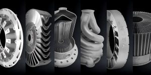
| Laser Powder Bed Fusion (LPBF / SLM) | Stainless Steel, Titanium Alloys, Aluminum Alloys | $0.5\text{ mm}$ to $0.8\text{ mm}$ | $1.0\text{ mm}$ to $1.5\text{ mm}$ | $20\ \mu\text{m}$ to $100\ \mu\text{m}$ | $\pm 50\ \mu\text{m}$ to $\pm 100\ \mu\text{m}$ | High-efficiency heat exchangers, engine manifolds, customized implants |
| Projection Micro Stereolithography ($\text{P}\mu\text{SL}$) | Photopolymers, Alumina & Zirconia Ceramics | $0.02\text{ mm}$ ($20\ \mu\text{m}$) | $0.05\text{ mm}$ ($50\ \mu\text{m}$) | $10\ \mu\text{m}$ to $50\ \mu\text{m}$ | $\pm 3\ \mu\text{m}$ (positional accuracy) | High-density chip sockets, microfluidic arrays, optical packaging |
| Two-Photon Polymerization (2PP) | Specialized IP-S & IP-n162 Photoresins | $0.0001\text{ mm}$ ($100\text{ nm}$) | $0.0005\text{ mm}$ ($500\text{ nm}$) | $0.1\ \mu\text{m}$ to $2.0\ \mu\text{m}$ | Sub-micron ($<100\text{ nm}$) | Micro-optics, on-fiber lenses, vascular tissue templates, MEMS |
III. Slicing Engines and Path Generation: How Software Redefines Physical Limits
Real-world feedback from engineering forums shows that slicer algorithms matter just as much as the hardware. Slicing software translates digital 3D designs into machine-readable toolpaths (G-code). In the past, FDM/FFF slicers used binary logic: features thinner than the nozzle diameter were ignored. If an engineer designed a $0.35\text{ mm}$ rib for a printer with a $0.4\text{ mm}$ nozzle, the print preview simply showed empty space.
The introduction of modern slicing engines—especially the Arachne wall generator (the default pathing engine in PrusaSlicer, OrcaSlicer, and Bambu Studio)—has completely changed this approach.
Legacy Slicer Pathing (Constant Bead Width)
[=== Nozzle Width ===] -> Drops paths thinner than nozzle diameter

Arachne Slicer Pathing (Variable Extrusion Width)
[=== Nozzle Width ===] -> Dynamically narrows volumetric flow to match CAD geometry
Arachne uses variable extrusion widths to scale the flow of melted polymer on the fly. In these modern slicers, the default minimum wall thickness is set to $85\%$ of the nominal nozzle diameter. Some operators on professional forums say you can push this down to $60\%$ (like printing a $0.24\text{ mm}$ wall with a $0.4\text{ mm}$ nozzle), but practical tests warn against doing this for structural parts.
The Risks of Pushing the 60% Volumetric Flow Limit
At $60\%$ nozzle width, print quality and consistency drop fast due to fluid dynamics inside the hotend:
- Nozzle Back-Pressure: Cutting the volumetric flow rate so drastically creates high back-pressure inside the heater block. This causes nozzle clogs, overheats the material, and leads to patchy under-extrusion.
- Layer Delamination: The resulting single-wall structures do not bond well because the polymer lacks the lateral pressure needed to form a flat, fully fused bead.
For B2B components that need predictable shear, tensile, and flexural strength, the basic engineering formula is:$$W_{\text{min}} \ge 2 \times D_{\text{nozzle}}$$
For a standard $0.4\text{ mm}$ nozzle, this keeps your wall threshold at $0.8\text{ mm}$. If you must print ultra-thin traces (like plastic-enclosed circuitry), swap to a smaller physical nozzle (such as a $0.2\text{ mm}$ nozzle) to keep your pathing width slightly wider than the nozzle’s inner bore. This step prevents internal voids and ensures high-density fusion.
IV. Material-Specific Wall Thickness Guidelines for CAD Designers
To help design engineers build robust CAD models, the table below lists the minimum and recommended wall thicknesses for common industrial materials. It also highlights the critical Structural Aspect Ratio (Height-to-Thickness Limit) to prevent parts from bending or buckling during production.
Material Performance Profile Matrix
| Feedstock Material Class | Manufacturing Technology | Minimum Wall Thickness | Recommended Structural Wall | Maximum Aspect Ratio (Height-to-Thickness) | Structural Mechanical Constraints |
|---|---|---|---|---|---|
| Standard PLA / ABS | FDM / FFF | $1.0\text{ mm}$ | $2.0\text{ mm}$ to $2.5\text{ mm}$ | $10:1$ | Anisotropic weakness; prone to splitting along layer lines under tension. |
| High-Precision ABS / PC | FDM / FFF | $1.5\text{ mm}$ | $3.0\text{ mm}$ | $12:1$ | High thermal shrinkage; thin features warp unless printed in a hot build chamber. |
| Flexible PLA / TPU | FDM / FFF | $2.0\text{ mm}$ | $4.0\text{ mm}$ to $5.0\text{ mm}$ | $4:1$ | High elasticity; thin vertical walls buckle under the weight and drag of the nozzle. |
| Polyamide (Nylon PA12) | SLS | $0.8\text{ mm}$ | $1.5\text{ mm}$ to $2.0\text{ mm}$ | $15:1$ | Prone to warping if cooled unevenly; absorbs moisture from the air. |
| Standard Resins | SLA / DLP | $0.8\text{ mm}$ | $1.5\text{ mm}$ to $2.0\text{ mm}$ | $15:1$ | Highly brittle; thin walls chip easily during support removal or final UV curing. |
| Tough / Specialty Resins | SLA / DLP | $1.0\text{ mm}$ | $2.0\text{ mm}$ | $18:1$ | Good impact resistance and ductility; useful for snap-fits and detailed casings. |
| Alumina / Zirconia Ceramics | $\text{P}\mu\text{SL}$ | $0.02\text{ mm}$ | $0.10\text{ mm}$ | $20:1$ | Great thermal stability; requires precise sintering shrinkage calculations in CAD. |
| Stainless Steel / Titanium | LPBF / SLM | $0.5\text{ mm}$ | $1.5\text{ mm}$ to $2.0\text{ mm}$ | $8:1$ | Severe internal stresses require heat treatment before removing parts from the build plate. |
V. High-Precision Miniaturization: B2B Industrial Case Studies
Let us look at three real-world case studies to see how these limits play out in practice.
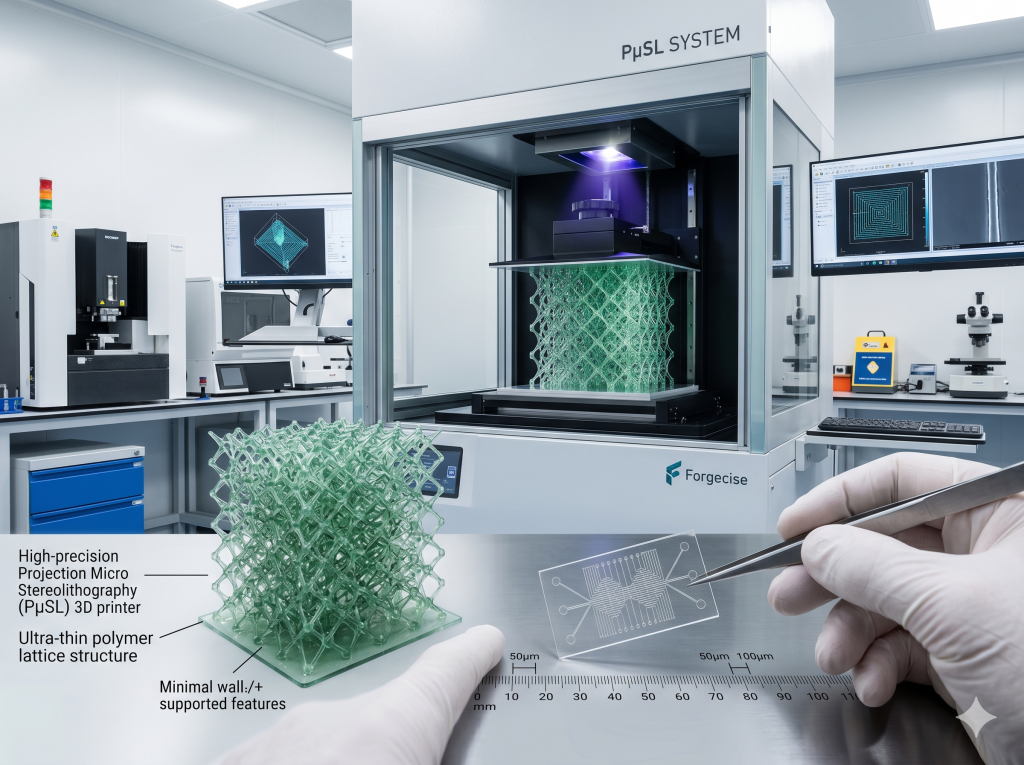
Case Study 1: High-Density Electronics: Hirose Electric and $\text{P}\mu\text{SL}$ Implementation
In the connector industry, product development cycles depend heavily on the speed of physical prototyping. Hirose Electric, a global manufacturer of electronic connectors used in smartphones and automotive ECUs, ran into a major bottleneck. Their prototype parts required micro-injection molds, which took $10\text{ to }12$ weeks to make and cost tens of thousands of dollars per revision.
Traditional Mold Cycle: 10 - 12 Weeks (High Tooling Cost) ──────────────────┐
                                                                           ▼
PμSL Prototyping Cycle: 1 - 2 Days (Zero Tooling Cost) ─────────► [Functional Verification]
To solve this, Hirose set up the BMF microArch S140 platform, which uses Projection Micro Stereolithography ($\text{P}\mu\text{SL}$). The target parts were circuit connectors measuring just a few millimeters wide and $1\text{ mm}$ tall. Crucially, the connector pins had functional holes spaced exactly $0.4\text{ mm}$ apart. If the thin walls separating these pin channels drifted by even a few microns, the metal terminals would not fit during assembly.
Using high-temperature, engineered photopolymer resins, the $\text{P}\mu\text{SL}$ system printed these connector housings with a positional accuracy of $\pm 3\ \mu\text{m}$. The parts matched the thermal and mechanical stability of injection-molded plastics during assembly testing. By swapping micro-injection molding for micro-AM, Hirose cut out tooling lead times entirely, shrinking design iterations from months to days while reducing initial R&D costs.
Case Study 2: Microfluidic Vascular Networks: ETH Zürich and Two-Photon Polymerization
Recreating three-dimensional microfluidic networks at biologically accurate scales is a difficult engineering challenge. Traditional photolithography is planar, which limits fluidic channels to flat, rectangular profiles that alter the shear stress of moving fluids compared to natural cylindrical blood vessels.
To bypass this barrier, researchers at ETH Zürich developed a hybrid additive manufacturing strategy. They used high-resolution Liquid-Crystal Display (LCD) 3D printing to make a macro-scale base microfluidic chip with integrated internal channels. Then, using Nanoscribe’s Two-Photon Polymerization (2PP) direct laser writing (DLW) system, they printed microvessels directly onto the chip’s microfluidic interface.
The 2PP system printed $100\ \mu\text{m}$ diameter polydimethylsiloxane (PDMS) microvessels with walls only $5\ \mu\text{m}$ thick. These ultra-thin walls featured arrays of pre-designed $5\ \mu\text{m}$ diameter micropores to allow physiological mass transfer (diffusion). The sub-micron accuracy of 2PP bypassed the optical distortion common to standard vat polymerization, showing a scalable path for organ-on-a-chip, pharmaceutical testing, and drug-screening platforms.
Case Study 3: Metallic Microlattices: Advanced Structural Replication
The physical limits of thin-walled metal printing are also tested in industrial R&D projects discussed within the professional AM community. In one case, a researcher tried to replicate a published scientific study on ultralight metallic microlattices using standard laboratory equipment.
The process began by printing a polymer lattice template on a high-precision SLA resin printer. This template was then coated using electroless plating, depositing roughly $10\ \mu\text{m}$ of nickel and $40\ \mu\text{m}\text{ to }50\ \mu\text{m}$ of copper. After coating, the internal polymer core was chemically dissolved, leaving behind a hollow metallic lattice with a final wall thickness of approximately $60\ \mu\text{m}$.
This project highlighted a critical non-linear mechanical scaling limit: while the original researchers produced resilient, elastic lattices with $10\ \mu\text{m}$ walls, the $60\ \mu\text{m}$ thick walls produced in this practical test made the lattice too stiff. Under compressive load, the thicker walls buckled plastically and failed to spring back.
This shows the delicate physics of thin-walled geometries: even a micro-scale increase in wall thickness can transition a structure from an elastic metamaterial to a rigid, brittle frame.
VI. Strategic Decision-Making Framework for B2B Procurement
For procurement officers and R&D directors, choosing the right AM technology is a balance between part requirements, lead times, and cost structures.
The Micro-AM Procurement Tree
To help B2B organizations, we have mapped out this technical decision framework:
                  Is the minimum design feature
                    or wall thickness < 0.5 mm?
                           /         \
                         YES          NO
                         /             \
           Is the minimum feature      Standard Industrial AM:
             or wall < 10 μm?          - FDM (Walls > 0.8 mm)
                /         \            - SLS (Walls > 0.8 mm)
              YES          NO          - SLA (Walls > 0.5 mm)
              /             \          - LPBF (Walls > 0.5 mm)
  Two-Photon Polymerization    Projection Micro Stereolithography
      (2PP - Nanoscribe)         (PμSL - Boston Micro Fabrication)
  - Core Applications:         - Core Applications:
    On-fiber micro-optics,       High-density electrical connectors,
    3D capillary networks,       disposable endoscope tips,
    photonic couplers.           microfluidic manifolds.
Production Volume Analysis: $\text{P}\mu\text{SL}$ vs. Micro Injection Molding
- Micro Injection Molding: This is the standard for high-volume production. However, it requires high upfront tooling costs (
$10{,}000\text{ to }50{,}000\ \text{USD}$) and long lead times ($10\text{ to }12$weeks) for mold design, CNC machining, and polishing. - Micro-AM ($\text{P}\mu\text{SL}$ / 2PP): This approach cuts out tooling costs entirely. It allows B2B companies to rapidly iterate designs, adjust geometries digitally, and transition to low-volume production (up to tens of thousands of parts) in a fraction of the time.
- The Hybrid Strategy: For production runs over
$100{,}000$units, companies can combine both worlds: use 2PP or $\text{P}\mu\text{SL}$ to 3D print a high-precision master template, then electroplate it to create a metal mold insert for high-volume injection molding.
VII. FAQ: Authoritative Solutions to Common Thin-Wall 3D Printing Questions
Q1: What are the mechanical trade-offs of using the Arachne slicer engine to scale thin vertical walls down to 60% of nozzle diameter?
Short Answer: Forcing a nozzle to print at $60\%$ width leads to high back-pressure, nozzle clogging, and weak layer-to-layer bonding.
Detailed Breakdown: The Arachne engine dynamically adjusts extrusion width, but forcing a $0.4\text{ mm}$ nozzle to print a $0.24\text{ mm}$ wall compromises structural integrity. When extrusion width drops far below the nozzle’s internal diameter, the polymer melt lacks the lateral compression required to form a flat, dense bead. This results in a rounded bead profile, creating microscopic voids between layers.
Furthermore, the reduced volumetric flow rate increases thermal dwell time inside the nozzle, leading to localized polymer degradation and low inter-layer shear strength. For load-bearing B2B enclosures or functional assemblies, keep the minimum wall thickness at $\ge 1.2 \times D_{\text{nozzle}}$ (e.g., $0.48\text{ mm}$ for a $0.4\text{ mm}$ nozzle) to ensure proper compression, complete bead fusion, and predictable mechanical performance.
Q2: Why do thin unsupported walls warp during the SLS sintering cycle, and how can over-sintering be prevented?
Short Answer: Localized heat builds up in the thin walls because the surrounding powder acts as an insulator, leading to thermal stress and uneven shrinkage.
Detailed Breakdown: SLS is a powder-bed fusion process that operates near the melting point of the polymer (e.g., PA12). When a laser scans a thin feature, localized thermal energy accumulates rapidly. For vertical walls designed below $0.45\text{ mm}$, this heat cannot dissipate through the surrounding unsintered powder, which acts as a thermal insulator.
This localized heat causes “over-sintering,” where adjacent unsintered powder particles fuse to the molten wall, resulting in dimensional swelling and high surface roughness. During the cooling cycle, these non-uniform, powder-dense boundaries contract unevenly, generating residual thermal stresses that warp or crack the wall.
To prevent over-sintering, unsupported walls must have a minimum thickness of $1.5\text{ mm}$. For supported walls, $0.8\text{ mm}$ to $1.0\text{ mm}$ is acceptable. Additionally, engineers must orient thin walls parallel to the recoater blade travel direction to minimize mechanical disruption during powder deposition.
Q3: What is the optimal strategy to prevent post-cure warp and structural collapse in thin-walled SLA/DLP photopolymer models?
Short Answer: Use high-molecular-weight tough resins, add structural bevels to your CAD design, and avoid printing flat surfaces parallel to the build plate.
Detailed Breakdown: During vat photopolymerization, printed parts exit the resin bath in a partially cured “green” state, retaining unreacted monomers within the cross-linked polymer network. Thinner walls (under $1.0\text{ mm}$) lack the flexural modulus to resist the localized volumetric shrinkage (typically $1\%\text{ to }3\%$) that occurs during final UV post-curing. Additionally, washing green parts in solvents like Isopropyl Alcohol (IPA) causes localized swelling, which induces stress cracking in thin-walled structures.
To mitigate this, B2B designers should use high-molecular-weight “tough” resins or mix in flexible additives (such as Siraya Tech Tenacious) to improve elastic deformation. In CAD, walls under $1.0\text{ mm}$ should incorporate a shallow bevel on non-visible surfaces to transition to a more stable $2.0\text{ mm}$ thickness.
Finally, for hollow structures, a minimum wall thickness of $2.5\text{ mm}$ should be used, and the build orientation should avoid large flat surfaces printed parallel to the build platform to minimize suction force damage during the peeling cycle.
Q4: Is it possible to print a completely hollow thin-walled sphere without internal supports in FDM, and what are the geometric limits of the top closure?
Short Answer: Yes, by using “spiralize vase mode” or adaptive layer slicing, but you must bridge the very top or print the sphere in two halves.
Detailed Breakdown: Printing a hollow, thin-walled sphere without support is governed by overhang angles and slicing constraints. As the printer builds the lower hemisphere, the overhang angle progresses from $0^\circ$ (vertical) to $90^\circ$ (horizontal). FDM systems can typically handle overhangs up to $45^\circ\text{ to }50^\circ$ without support. Beyond this angle, successive layers are deposited partially in the air, leading to layer sagging and poor surface finish. Near the top of the sphere, the layer path is deposited entirely over empty space, causing complete print failure.
To print a hollow sphere without supports, engineers can use “spiralize vase mode,” which prints a single continuous extrusion path with zero infill and no retraction, minimizing warping. However, to successfully close the top dome, the design must incorporate a flat bridging spot on the interior ceiling, or use adaptive layer height slicing to reduce layer thickness at the top. This increases layer overlap and allows the bead to bridge the gap successfully. For functional parts, the most reliable approach is to print the sphere in two halves and bond them post-print.
Q5: How do B2B companies choose between micro injection molding and micro-precision 3D printing ($\text{P}\mu\text{SL}$) for production connectors and medical components?
Short Answer: Micro injection molding is best for high volumes (over 100k parts), while micro-AM is ideal for rapid prototyping and low-volume production runs.
Detailed Breakdown: The decision between micro injection molding and micro-AM depends on production volume, lead time, and material requirements. Micro injection molding is the standard for high-volume production, but requires significant upfront tooling costs ($10{,}000\text{ to }50{,}000\ \text{USD}$) and long lead times ($10\text{ to }12$ weeks).
$\text{P}\mu\text{SL}$ micro-AM systems, such as the BMF microArch S150, eliminate tooling entirely. This allows B2B companies to rapidly iterate designs and transition to low-volume production (up to tens of thousands of parts) in a fraction of the time.
Additionally, $\text{P}\mu\text{SL}$ systems achieve positional accuracy of $\pm 3\ \mu\text{m}$ and can print in engineering-grade resins and ceramics, matching the resolution and thermal stability of molded plastics. For production volumes exceeding $100{,}000$ units, the optimal strategy is a hybrid approach: use 2PP or $\text{P}\mu\text{SL}$ to 3D print a high-precision master template, and electroplate it to create a mold insert for high-volume injection molding.
VIII. Designing for the Micro-AM Era
You can bypass the physical limits of thin-wall printing if you align your CAD geometry with your hardware’s thermal behavior. As B2B manufacturing transitions from large assemblies to integrated micro-systems, mastering layer heights, slicing engines, and material traits becomes essential for development teams.
By utilizing clear design guidelines and strategic procurement setups, R&D teams can use micro-AM to reduce lead times, save on material, and bring products to market faster.
About the Author
Felix Lee is the CEO of Forgecise, a strategic consultancy specializing in additive manufacturing pipelines for semiconductor and medical technology companies. With over 15 years of experience in advanced manufacturing, Felix works at the intersection of material science and mechanical hardware limits, helping B2B organizations implement micro-fabrication technology. Contact Felix or the Forgecise analysis team for technical consultations and hardware integration strategies.